With Huawei’s major release of the “Tao (τ) Law” on May 25 this year, replacing traditional “geometric scaling” with “time scaling,” the industry is continuously reducing signal propagation latency and greatly increasing transistor density. This officially opens a new era in which China’s semiconductor industry moves from “following rules” toward “leading paradigms.” At the same time, five departments including the National Development and Reform Commission have continued to increase tax incentive support for 2026, and semiconductor inspection equipment has been clearly included in the “15th Five-Year Plan” strategic emerging industry breakthrough list. The triple momentum of “surging demand + stronger policy support + accelerated domestic substitution” has created an important window for the rapid breakthrough of China’s independently developed semiconductor test equipment.
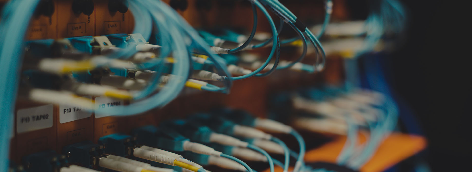
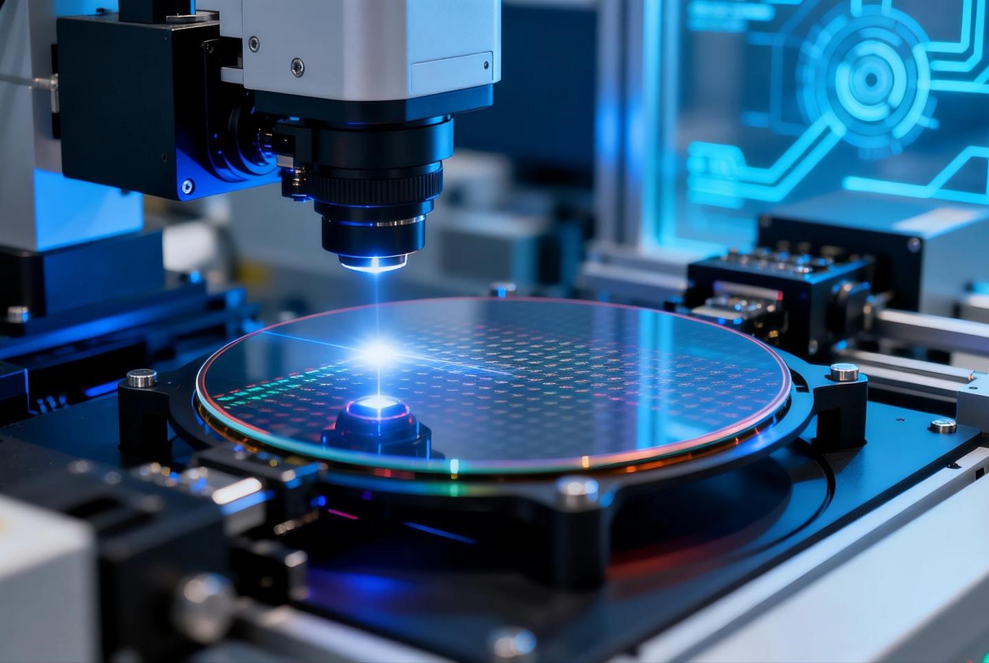
Driven by both industrial transformation and national policy, semiconductor wafer inspection equipment, as the yield-control infrastructure spanning chip design, wafer manufacturing, packaging, and testing, is entering a resonance period of “global recovery + accelerated domestic substitution.” As semiconductor processes advance toward the nanometer and even atomic scale, tiny defects on wafer surfaces, such as scratches, particles, pits, and contaminants, have an increasingly critical impact on chip yield. In wafer inspection, automated optical inspection (AOI) equipment must process massive volumes of high-resolution image data in real time, placing stringent requirements on the computing power, expandability, stability, and environmental adaptability of the core computing unit.
A domestic solution provider specializing in semiconductor inspection equipment needed its wafer defect inspection equipment to meet high cleaning standards while enabling high-speed synchronized acquisition from multiple cameras, real-time operation of AI defect recognition algorithms, and 24/7 uninterrupted production. Accordingly, the customer defined clear requirements for the core industrial computer.
Customer Challenge
In the customer’s wafer inspection equipment upgrade project, the following core challenges were identified:
1. High-precision real-time inspection requirements: The system needed to simultaneously process wafer surface images captured by multiple high-resolution industrial cameras and identify micron-level defects such as scratches, particles, and stains in real time.
2. Insufficient expandability: The equipment needed to connect multiple industrial cameras, motion control cards, data acquisition cards, light source controllers, and other PCIe/PCI devices at the same time.
3. Stability and reliability: Semiconductor production lines require 24/7 continuous operation, and any unexpected downtime can cause major losses. The equipment also needed to adapt to wafer-fab cleanroom environments compliant with ISO 14644-1 and provide strict ESD protection.
4. Data security requirements: Inspection data needed to be retained for the long term, with RAID array support to prevent data loss caused by a single-drive failure.
APQ Solution
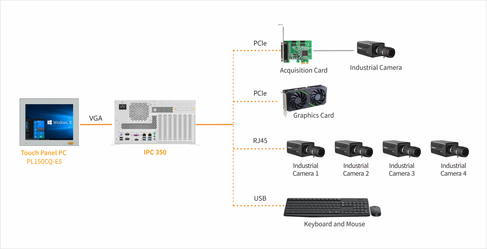
Based on these requirements, APQ provided the customer with a wafer defect inspection solution using the IPC350-Q670SA2 wall-mounted wafer inspection industrial computer as the core computing unit. The solution offers the following key advantages:
01 Powerful computing performance for real-time inspection
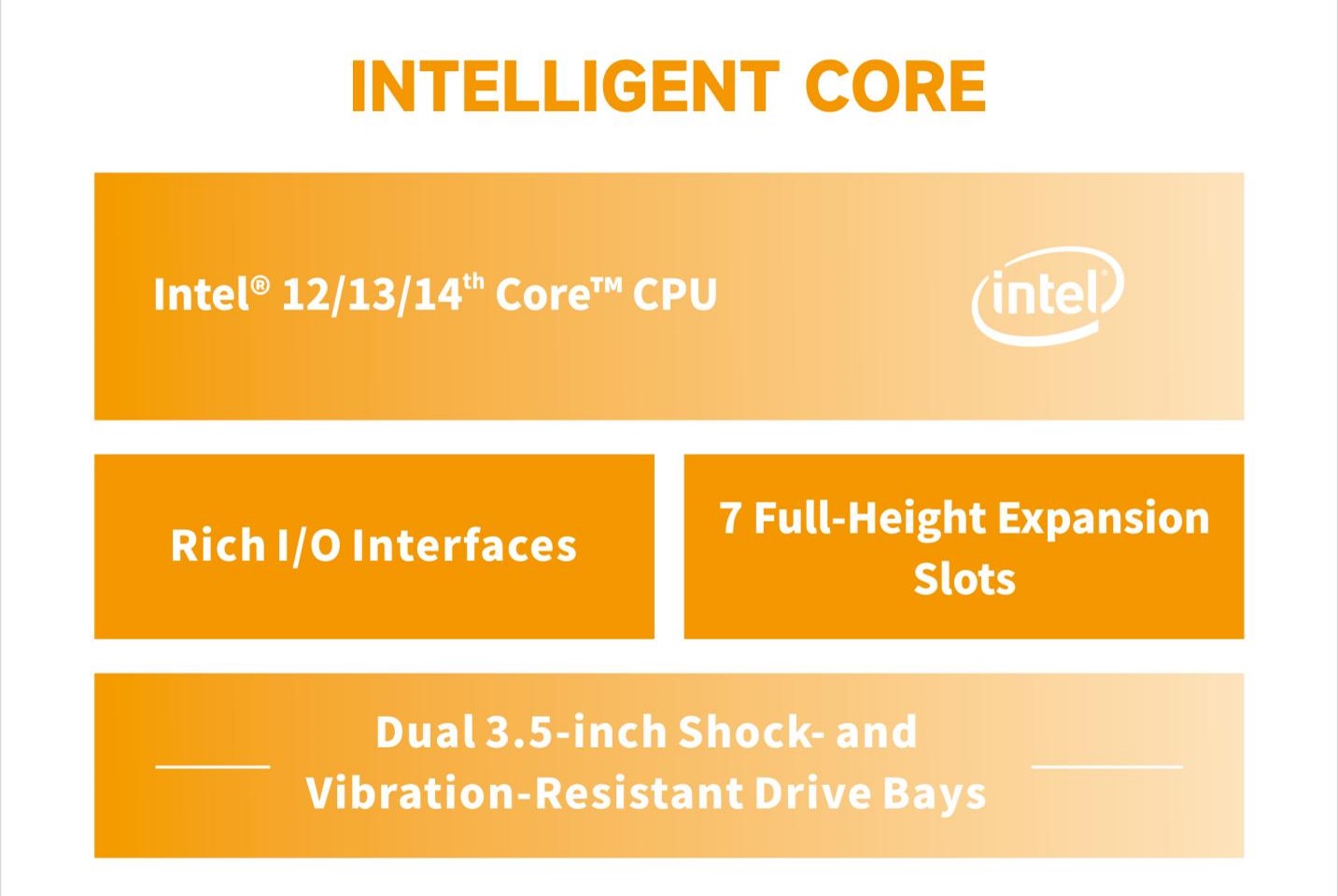
The IPC350-Q670SA2 is equipped with Intel® 12th/13th/14th Gen Core/Pentium/Celeron desktop CPUs and 4 × DDR5 memory slots, supporting up to 192 GB. It can easily handle real-time processing of massive image data and parallel inference for complex vision algorithms in wafer inspection scenarios. Whether identifying tiny surface scratches or analyzing nanoscale crystal defects, it provides the computing support needed for real-time response.
02 Extensive expansion for multiple inspection schemes
7 full-height expansion slots: including 2 × PCIe x16, 3 × PCIe x4, and 2 × PCI, meeting the need to connect multiple high-speed cameras, motion control cards, and GPU acceleration cards simultaneously in wafer inspection equipment.
1 × M.2 Key-E supports Wi-Fi/Bluetooth modules for easy wireless expansion.
The tool-free PCIe expansion card retainer uses a highly vibration-resistant design suitable for the slight vibration environment of wafer-fab workshops.
03 Rich I/O interfaces to simplify system integration
Rear: 2 × RJ45 Gigabit Ethernet ports, 6 × USB 5 Gbps, 1 × RS232, and independent triple-display output via HDMI/VGA/DVI-D, supporting simultaneous connection of light source controllers, cameras, monitors, and PLCs.
Front: 2 × USB, power switch, and status indicators for easier on-site debugging and maintenance.
Internal: 5 × USB, 5 × COM ports with optional RS232/485/422, and 8-channel GPIO, allowing connection to various sensors and actuators without additional expansion and significantly reducing system integration complexity.
04 Industrial-grade reliability for harsh environments
The fully galvanized steel chassis effectively shields electromagnetic interference and works with the grounding design to provide basic ESD protection.
Independent airflow design: intelligent cooling with a CPU fan and system fan, supporting an operating temperature range of 0-50°C and maintaining thermal stability even under long-duration, high-load inspection.
Dual 3.5-inch shock-resistant drive bays support hybrid deployment of high-speed SSDs and large-capacity HDDs, meeting requirements for long-term inspection data retention and secure backup, with configurable RAID arrays.
The compact small 4U chassis, measuring 330 × 351 × 180 mm, supports both wall-mounted and desktop installation, flexibly adapting to different inspection equipment layouts.
Value Achievements:
By introducing the APQ IPC350-Q670SA2, the semiconductor inspection equipment solution provider successfully achieved the following:
Significantly improved inspection efficiency:
The combination of a high-performance CPU and large-capacity memory improves the operating efficiency of AI defect recognition algorithms, enabling wafer inspection throughput to meet production line requirements.
Reduced system integration complexity: Seven full-height expansion slots and rich I/O interfaces enable one-machine integration of cameras, acquisition cards, motion cards, PLCs, and other devices, simplifying the system architecture and improving overall machine reliability.
Assured continuous production: Industrial-grade reliability, intelligent cooling, and RAID-based data security mechanisms ensure stable 24/7 operation in cleanroom environments, keeping the monthly failure rate extremely low.
Flexible deployment and space savings: The small 4U chassis supports wall-mounted installation and can be flexibly integrated into compact inspection equipment cabinets, giving customers greater freedom in production line layout.
Post time: Jun-04-2026


